- 您现在的位置:买卖IC网 > Sheet目录1233 > NCP1608BOOSTGEVB (ON Semiconductor)BOARD EVAL NCP1608 100W BOOST
�� �
�
�NCP1608�
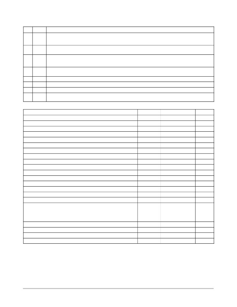
�Table� 1.� PIN� FUNCTION� DESCRIPTION�
�Pin�
�1�
�2�
�3�
�4�
�5�
�6�
�7�
�8�
�Name�
�FB�
�Control�
�Ct�
�CS�
�ZCD�
�GND�
�DRV�
�V� CC�
�Function�
�The� FB� pin� is� the� inverting� input� of� the� internal� error� amplifier.� A� resistor� divider� scales� the� output� voltage� to� V� REF� to� main-�
�tain� regulation.� The� feedback� voltage� is� used� for� overvoltage� and� undervoltage� protections.� The� controller� is� disabled�
�when� this� pin� is� forced� to� a� voltage� less� than� V� UVP� ,� a� voltage� greater� than� V� OVP� ,� or� floating.�
�The� Control� pin� is� the� output� of� the� internal� error� amplifier.� A� compensation� network� is� connected� between� the� Control� pin�
�and� ground� to� set� the� loop� bandwidth.� A� low� bandwidth� yields� a� high� power� factor� and� a� low� Total� Harmonic� Distortion� (THD).�
�The� Ct� pin� sources� a� current� to� charge� an� external� timing� capacitor.� The� circuit� controls� the� power� switch� on� time� by� com-�
�paring� the� Ct� voltage� to� an� internal� voltage� derived� from� V� Control� .� The� Ct� pin� discharges� the� external� timing� capacitor� at� the�
�end� of� the� on� time.�
�The� CS� pin� limits� the� cycle� ?� by� ?� cycle� current� through� the� power� switch.� When� the� CS� voltage� exceeds� V� ILIM� ,� the� drive�
�turns� off.� The� sense� resistor� that� connects� to� the� CS� pin� programs� the� maximum� switch� current.�
�The� voltage� of� an� auxiliary� winding� is� sensed� by� this� pin� to� detect� the� inductor� demagnetization� for� CrM� operation.�
�The� GND� pin� is� analog� ground.�
�The� integrated� driver� has� a� typical� source� impedance� of� 12� W� and� a� typical� sink� impedance� of� 6� W� .�
�The� V� CC� pin� is� the� positive� supply� of� the� controller.� The� controller� is� enabled� when� V� CC� exceeds� V� CC(on)� and� is� disabled�
�when� V� CC� decreases� to� less� than� V� CC(off)� .�
�Table� 2.� MAXIMUM� RATINGS�
�Rating�
�FB� Voltage�
�FB� Current�
�Control� Voltage�
�Control� Current�
�Ct� Voltage�
�Ct� Current�
�CS� Voltage�
�CS� Current�
�ZCD� Voltage�
�ZCD� Current�
�DRV� Voltage�
�DRV� Sink� Current�
�DRV� Source� Current�
�Supply� Voltage�
�Supply� Current�
�Power� Dissipation� (T� A� =� 70� °� C,� 2.0� Oz� Cu,� 55� mm� 2� Printed� Circuit� Copper� Clad)�
�Thermal� Resistance� Junction� ?� to� ?� Ambient�
�(2.0� Oz� Cu,� 55� mm� 2� Printed� Circuit� Copper� Clad)�
�Junction� ?� to� ?� Air,� Low� conductivity� PCB� (Note� 3)�
�Junction� ?� to� ?� Air,� High� conductivity� PCB� (Note� 4)�
�Operating� Junction� Temperature� Range�
�Maximum� Junction� Temperature�
�Storage� Temperature� Range�
�Lead� Temperature� (Soldering,� 10� s)�
�Symbol�
�V� FB�
�I� FB�
�V� Control�
�I� Control�
�V� Ct�
�I� Ct�
�V� CS�
�I� CS�
�V� ZCD�
�I� ZCD�
�V� DRV�
�I� DRV(sink)�
�I� DRV(source)�
�V� CC�
�I� CC�
�P� D�
�R� q� JA�
�R� q� JA�
�R� q� JA�
�T� J�
�T� J(MAX)�
�T� STG�
�T� L�
�Value�
�?� 0.3� to� 10�
�±� 10�
�?� 0.3� to� 6.5�
�?� 2� to� 10�
�?� 0.3� to� 6�
�±� 10�
�?� 0.3� to� 6�
�±� 10�
�?� 0.3� to� 10�
�±� 10�
�?� 0.3� to� V� CC�
�800�
�500�
�?� 0.3� to� 20�
�±� 20�
�450�
�178�
�168�
�127�
�?� 40� to� 125�
�150�
�?� 65� to� 150�
�300�
�Unit�
�V�
�mA�
�V�
�mA�
�V�
�mA�
�V�
�mA�
�V�
�mA�
�V�
�mA�
�mA�
�V�
�mA�
�mW�
�°� C/W�
�°� C�
�°� C�
�°� C�
�°� C�
�Stresses� exceeding� Maximum� Ratings� may� damage� the� device.� Maximum� Ratings� are� stress� ratings� only.� Functional� operation� above� the�
�Recommended� Operating� Conditions� is� not� implied.� Extended� exposure� to� stresses� above� the� Recommended� Operating� Conditions� may� affect�
�device� reliability.�
�1.� This� device� series� contains� ESD� protection� and� exceeds� the� following� tests:�
�Pins� 1–� 8:� Human� Body� Model� 2000� V� per� JEDEC� Standard� JESD22� ?� A114E.�
�Pins� 1–� 8:� Machine� Model� Method� 200� V� per� JEDEC� Standard� JESD22� ?� A115� ?� A.�
�2.� This� device� contains� Latch� ?� Up� protection� and� exceeds� ±� 100� mA� per� JEDEC� Standard� JESD78.�
�3.� As� mounted� on� a� 40x40x1.5� mm� FR4� substrate� with� a� single� layer� of� 80� mm� 2� of� 2� oz� copper� traces� and� heat� spreading� area.� As� specified� for�
�a� JEDEC� 51� low� conductivity� test� PCB.� Test� conditions� were� under� natural� convection� or� zero� air� flow.�
�4.� As� mounted� on� a� 40x40x1.5� mm� FR4� substrate� with� a� single� layer� of� 650� mm� 2� of� 2� oz� copper� traces� and� heat� spreading� area.� As� specified�
�for� a� JEDEC� 51� high� conductivity� test� PCB.� Test� conditions� were� under� natural� convection� or� zero� air� flow.�
�http://onsemi.com�
�3�
�发布紧急采购,3分钟左右您将得到回复。
相关PDF资料
NCP1631PFCGEVB
BOARD DEMO NCP1631 INTERLEAV PFC
NCP1650EVB
BOARD EVAL NCP1650 PFC CTLR
NCP1652L48VGEVB
BOARD EVAL 100W 48V NCP1652 PFC
NCP1653EVB
BOARD EVAL FOR NCP1653
NCP2993FCT2GEVB
BOARD EVAL NCP2993 AUDIO PWR AMP
NCP345SNT1G
IC DETECTOR OVER VOLTAGE 5TSOP
NCP346SN2T1G
IC DETECTOR OVER VOLTAGE 5TSOP
NCP347MTAITBG
IC OVERVOLTAGE PROT CTRLR 10WDFN
相关代理商/技术参数
NCP1611ADR2G
功能描述:功率因数校正 IC NCP1611A ENHANCED PFC
RoHS:否 制造商:Fairchild Semiconductor 开关频率:300 KHz 最大功率耗散: 最大工作温度:+ 125 C 安装风格:SMD/SMT 封装 / 箱体:SOIC-8 封装:Reel
NCP1611BDR2G
功能描述:功率因数校正 IC NCP1611A ENHANCED PFC RoHS:否 制造商:Fairchild Semiconductor 开关频率:300 KHz 最大功率耗散: 最大工作温度:+ 125 C 安装风格:SMD/SMT 封装 / 箱体:SOIC-8 封装:Reel
NCP1611GEVB
制造商:ON Semiconductor 功能描述:PG - ACDC CONVERSION - Bulk 制造商:ON Semiconductor 功能描述:EVAL BOARD, NCP1611, POWER FACTOR CORRECTION; Silicon Manufacturer:On Semiconductor; Silicon Core Number:NCP1611; Kit Application Type:Power Management; Application Sub Type:Power Factor Correction (PFC) ;RoHS Compliant: Yes
NCP1612ADR2G
功能描述:功率因数校正 IC
RoHS:否 制造商:Fairchild Semiconductor 开关频率:300 KHz 最大功率耗散: 最大工作温度:+ 125 C 安装风格:SMD/SMT 封装 / 箱体:SOIC-8 封装:Reel
NCP1612BDR2G
制造商:ON Semiconductor 功能描述:ENHANCED HIGH-EFFICIENCY - Tape and Reel
NCP1612GEVB
制造商:ON Semiconductor 功能描述:PG - ACDC CONVERSION - Bulk 制造商:ON Semiconductor 功能描述:EVAL BOARD, NCP1612, POWER FACTOR CORRECTION; Silicon Manufacturer:On Semiconductor; Silicon Core Number:NCP1612; Kit Application Type:Power Management; Application Sub Type:Power Factor Correction (PFC) ;RoHS Compliant: Yes
NCP1615ADR2G
制造商:ON Semiconductor 功能描述:HV HIGH EFFICIENCY PFC CO - Tape and Reel
NCP1631DR2G
功能描述:功率因数校正 IC 2 PHASE INTERLEAVE PFC RoHS:否 制造商:Fairchild Semiconductor 开关频率:300 KHz 最大功率耗散: 最大工作温度:+ 125 C 安装风格:SMD/SMT 封装 / 箱体:SOIC-8 封装:Reel